Small Signal Model
Contents
Small Signal Model#
Building up the model#
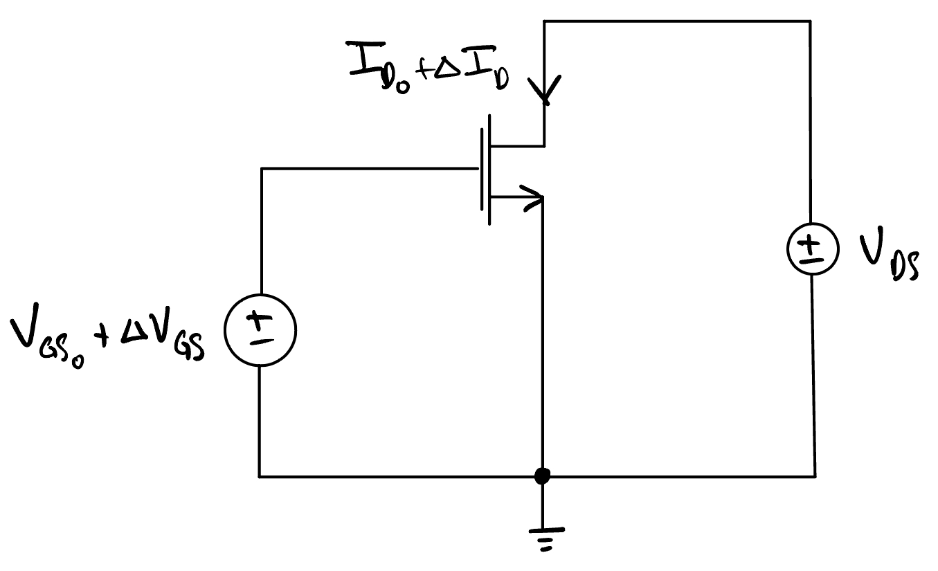
Fig. 15 Small-signal model where the signal is added to the gate.#
Since these models are so nonlinear, we linearize around specific bias points. The \(\Delta I_D\) and \(\Delta V_{\text{GS}}\) is the signal riding on top of the large signal, \(V_{\text{GS}_0}\) and \(I_{D_0}\).
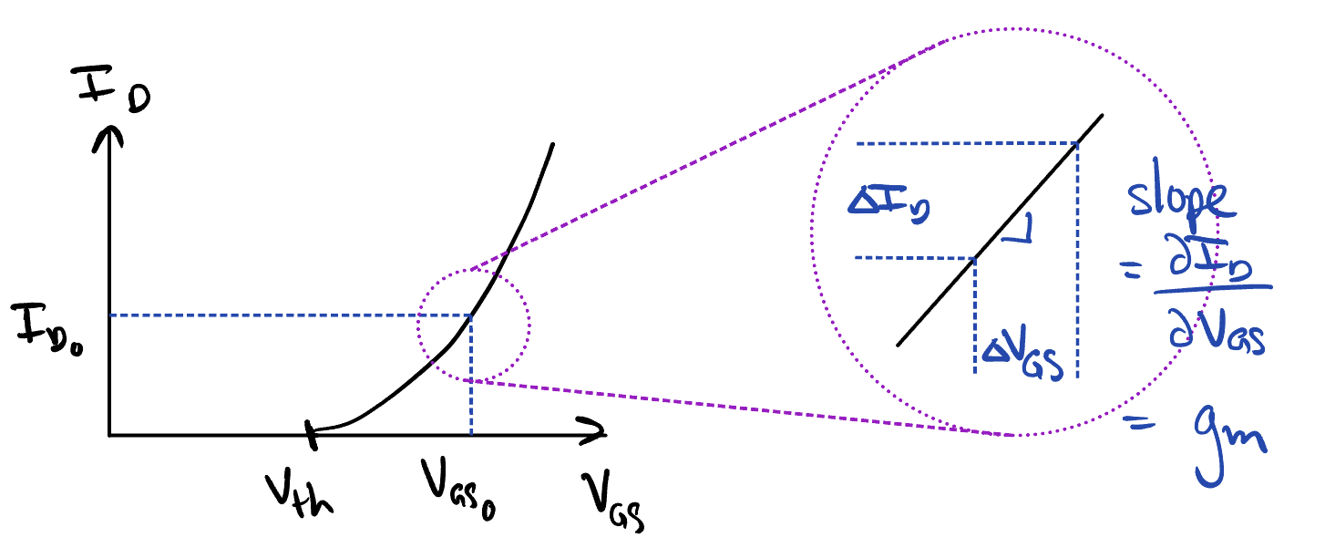
Fig. 16 Linearization of the IV curve.#
In the above figure, \(\Delta V_{\text{GS}}\) and the operating point are added to the signal \(V_{\text{GS}_0}\).
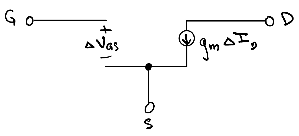
Fig. 17 Small-signal equivalent circuit.#
In the above figure, \(\Delta I_D = g_m \Delta V_{\text{GS}}\).
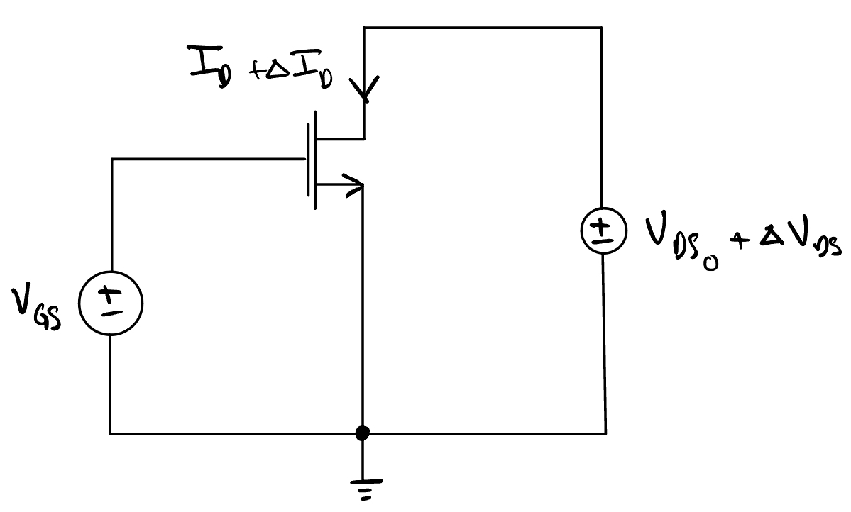
Fig. 18 Small-signal model where the signal is added to the drain.#
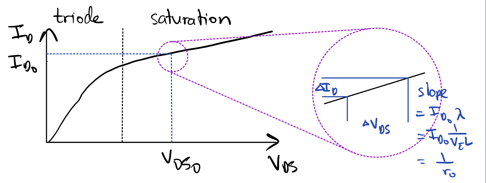
Fig. 19 Linearization of the IV curve.#
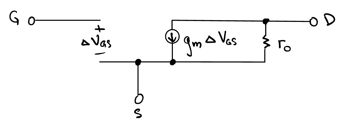
Fig. 20 Small-signal model adds the resistor to include the channel length modulation effect.#
Note the addition of the resistor \(R_0\) in the above circuit. This includes the effects of channel length modulation into the small-signal mode and models the change in \(I_D\) in response to the change in \(V_{\text{DS}}\).

Fig. 21 We normally connect bulk to the lowest voltage to avoid any current flow.#
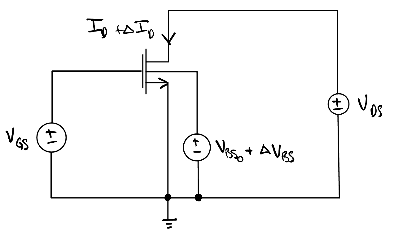
Fig. 22 We can bias the MOSFET to saturation.#
where \(\eta \approxeq 0.2\), typically. We often set \(g_{\text{mb}}\) to 0, since its effects are 5x smaller.
NMOS model#
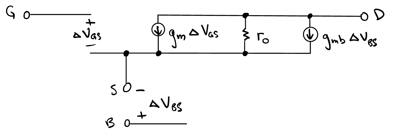
Fig. 23 Small-signal model of an NMOS.#
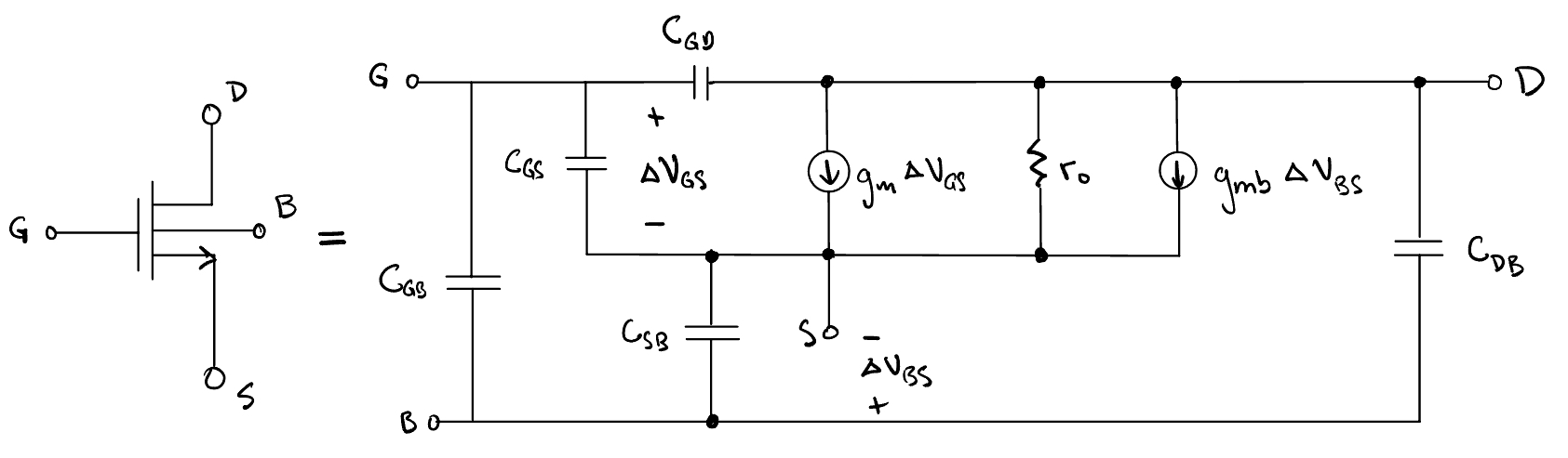
Fig. 24 Complete NMOS model with capacitances.#
PMOS model#
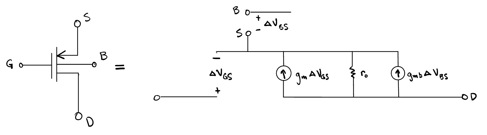
Fig. 25 Small-signal model of a PMOS.#
Summary#
Region of Operation |
Condition |
|---|---|
Cutoff |
\(V_{\text{SG}} \lt V_{\text{th}}\) |
Saturation |
\(V_{\text{SD}} \gt V_{\text{SG}}, V_{\text{SG}} \geq V_{\text{th}}\) |
Triode |
\(V_{\text{SD}} \leq V_{\text{SG}} - V_{\text{th}}, V_{\text{SG}} \geq V_{\text{th}}\) |