Current Mirrors
Contents
Current Mirrors#
Current mirrors#
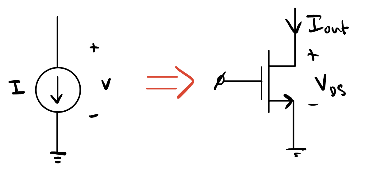
Fig. 77 Diode-connected PMOS load.#
In the above circuit, \(I_{\text{out}}\) is given by
We can use current mirrors to create current sources, since \(I_{\text{out}}\) is a weak function of \(V_{DS}\). In saturation, \(I_{\text{out}}\) is essentially independent of voltage (see Figure 13). Channel-length modulation, which is often ignored, is the only factor changing current in saturation.
How do we produce well-defined \(I_{\text{out}}\) then?
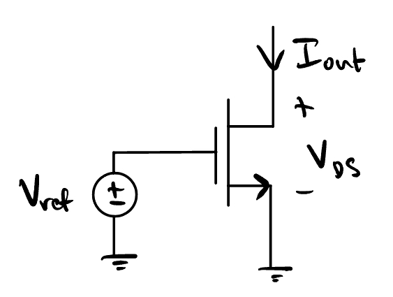
Fig. 78 In this configuration, \(I_{\text{out}}\) is sensitive to PVT/device parameters.#
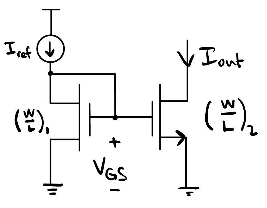
Fig. 79 In this configuration, \(I_{\text{out}}\) is independent of PVT/device parameters.#
In Figure 79, \(I_{\text{out}}\) is given by
and
Substituting gives
This will give an \(I_{\text{out}}\) that is independent of device parameters. The ratio of two \(W/L\)’s can be very accurate if the devices are close together.
Note that discrete components won’t necessarily work because they come from different wafers and have different coefficients. But when devices are close together, it’s normal for errors to affect both \(W/L_1\) and \(W/L_2\) equally, cancelling out the effect. The ratios can be made very precise.
Effect of channel-length modulation#
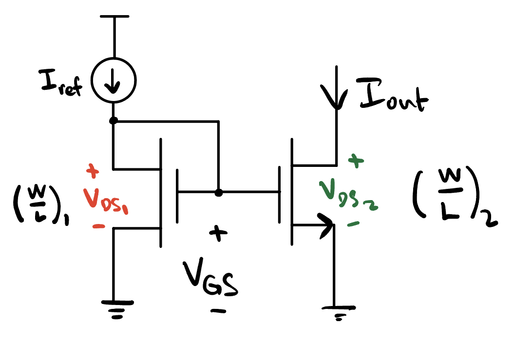
Fig. 80 Effects of channel-length modulation. \(I_{\text{out}} = I_{\text{ref}}\) only if \(V_{\text{DS}_1} = V_{\text{DS}_2}\).#
If \(V_{\text{DS}_1} \ne V_{\text{DS}_2}\), \(I_{\text{out}}\) will suffer an error. You can, however, use a larger \(\lambda = V_E L / I_D\) to reduce the error.
Cascode current mirrors#
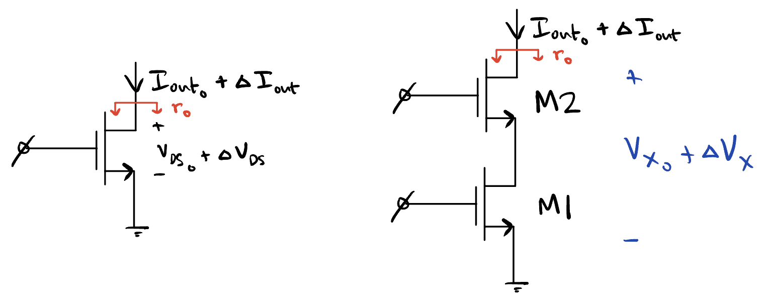
Fig. 81 Cascode current mirrors. The case on the right acts more like an ideal current source.#
In the case of the left circuit,
but in the case of the right,
because the output impedance of a cascode amp, the \(r_o\) of the circuit on the right, is
where \((g_{m_2} + g_{mb_1}) {r_{o_2} r_{o_1}} \gg 1\). Therefore, the second case (on the right) is the more ideal current source.
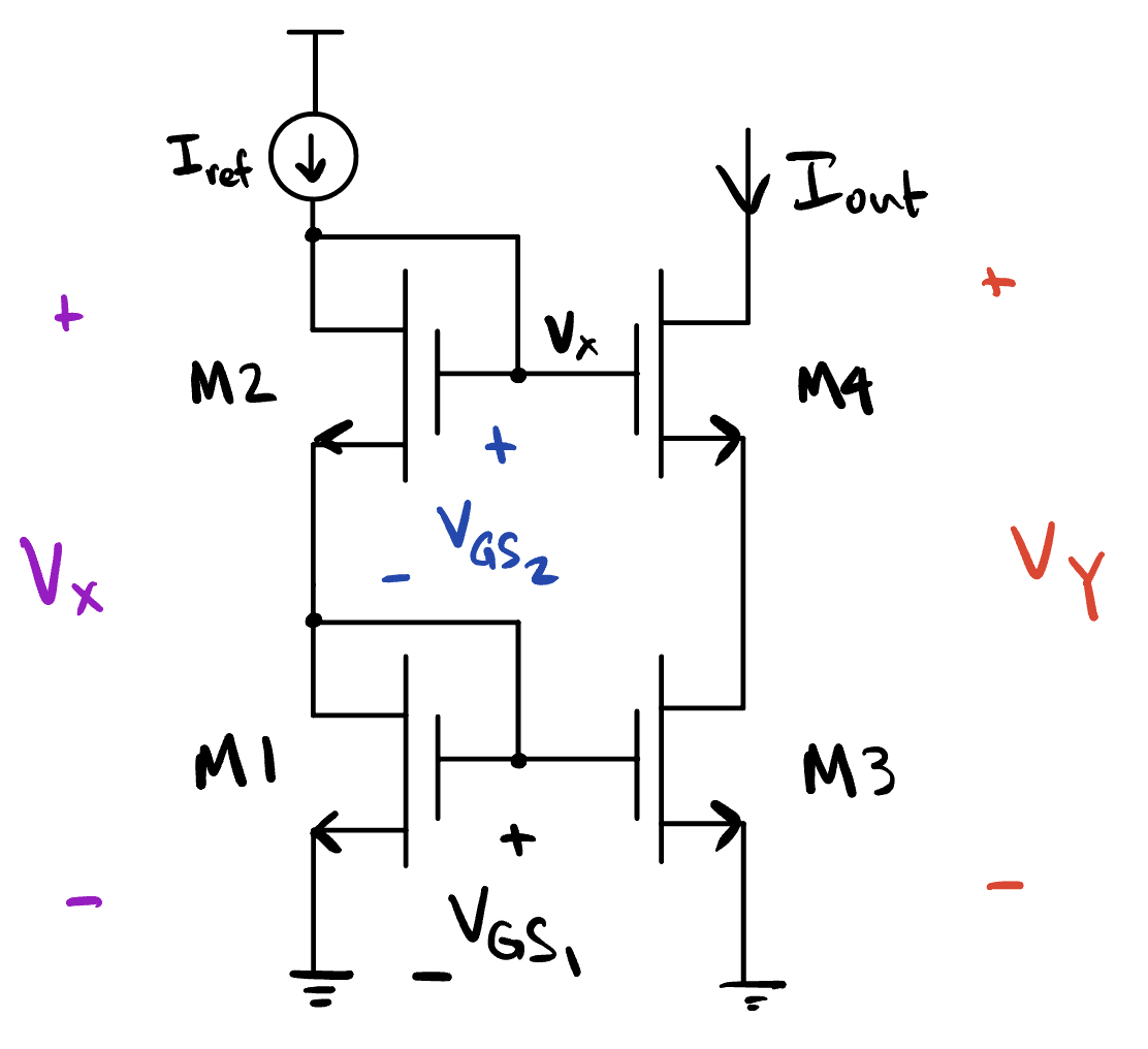
Fig. 82 Mismatch between \(V_X\) and \(V_Y\).#
In the above, \(V_X = V_{\text{GS}_1} + V_{\text{GS}_2} \gt 2 V_{\text{th}}\). If \(V_Y\) is too small, M4 will go into triode. Therefore, \(V_Y \ge V_X - V_{\text{th}}\) for M4 to be in saturation.
In this circuit, \(I_{\text{out}}\) is less sensitive to mismatch between \(V_X\) and \(V_Y\).
Which \(W/L\)’s define \(I_{\text{out}}\)?
What is the minimum \(V_Y\) before M3, M4 go into triode?
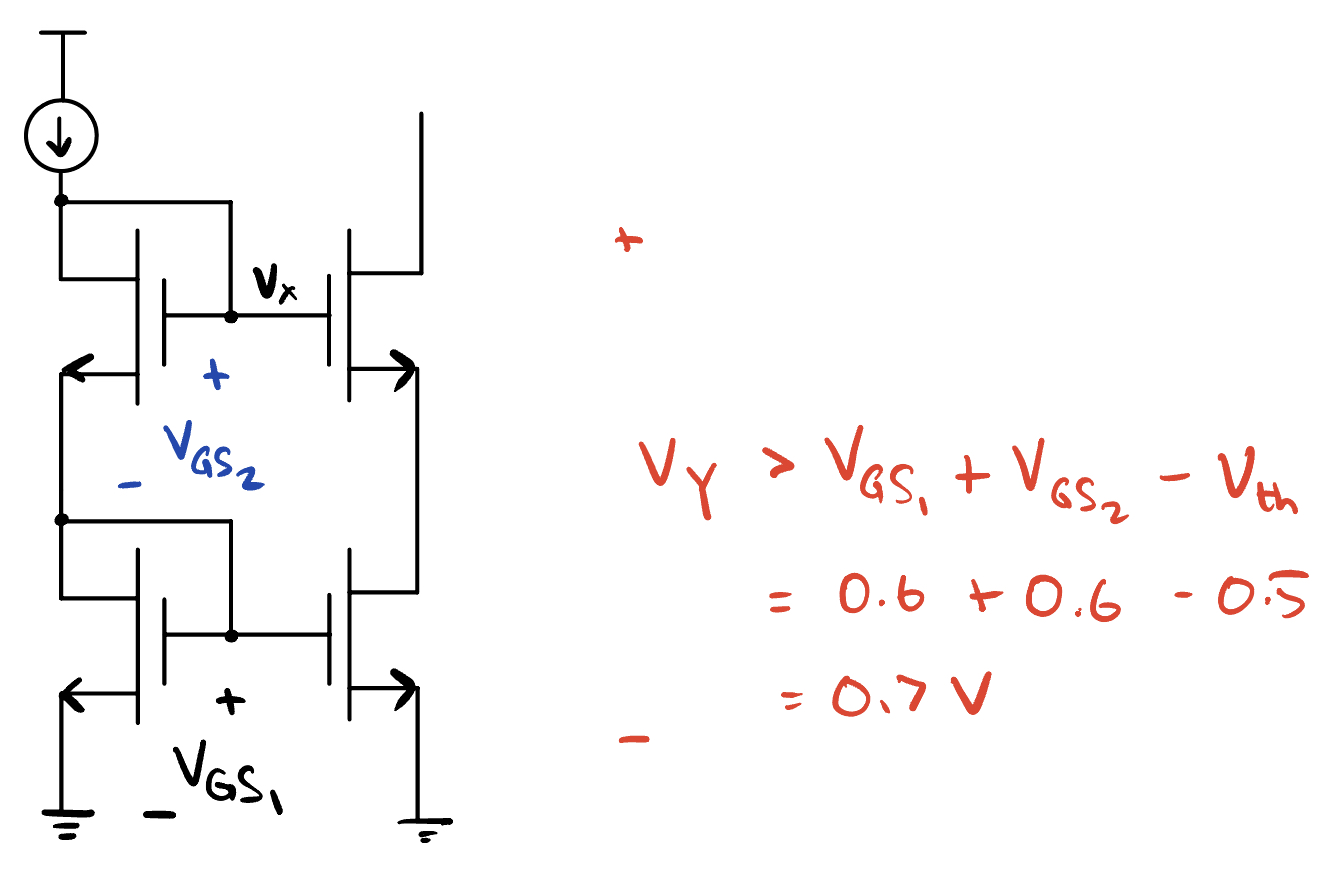
Fig. 83 \(V_Y\) requires a relatively high voltage to remain in saturation, so this topology is not good when you only have a low supply voltage.#
Wide-swing cascode current mirrors#
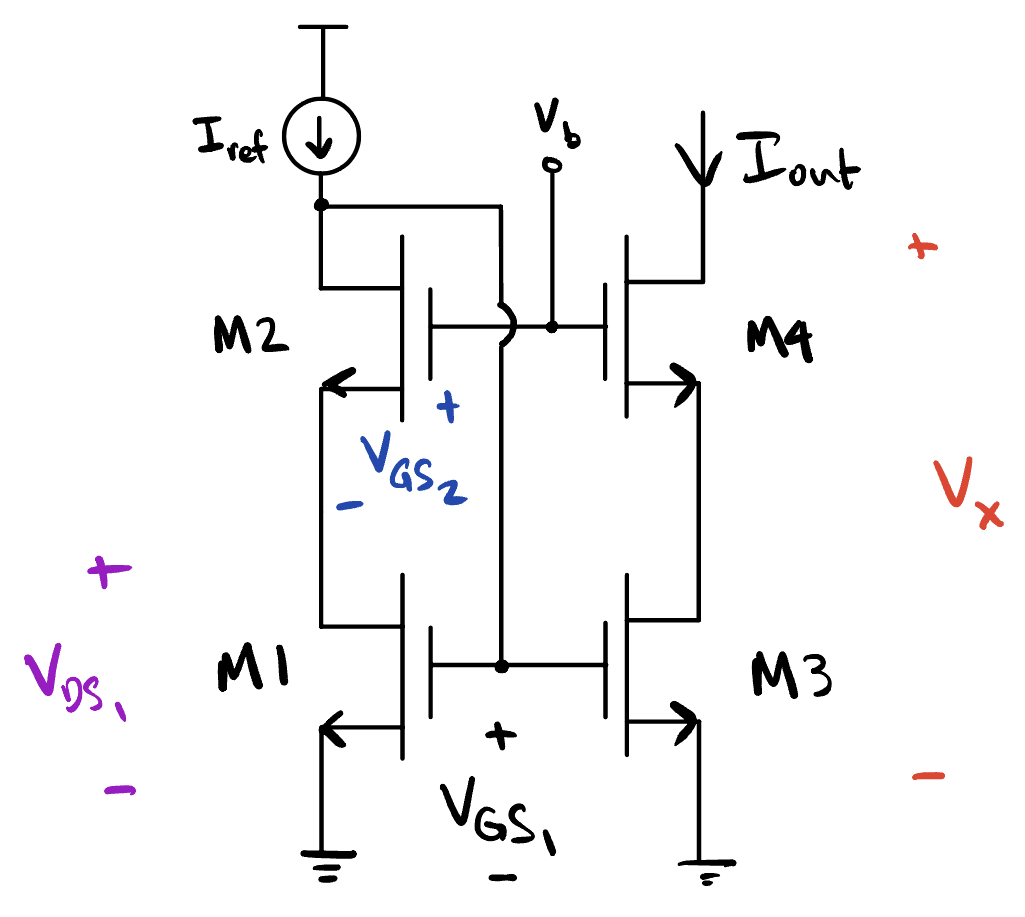
Fig. 84 Wide-swing cascode current mirrors.#
In this configuration, \(V_{\text{DS}_1} \ge V_{\text{GS}} - V_{\text{th}}\) for M1 to be in saturation. Additionally,
is the lower bound on \(V_b\) to keep M1 out of triode. Also, to keep M4 in saturation, \(V_X \ge V_b - V_{\text{th}}\).
\(V_{\text{GS}_1} \ge V_b - V_{\text{th}}\) is a requirement for M2 to be in saturation, and \(V_b \le V_{\text{GS}_1} + V_{\text{th}}\) is an upper bound on \(V_b\).
As an example,
we can see that \(V_X\) can be as low as \(0.2\) and keep all MOSFETs in saturation! Now you can use a one volt supply and still have headroom.
Differential amp with current mirror load#
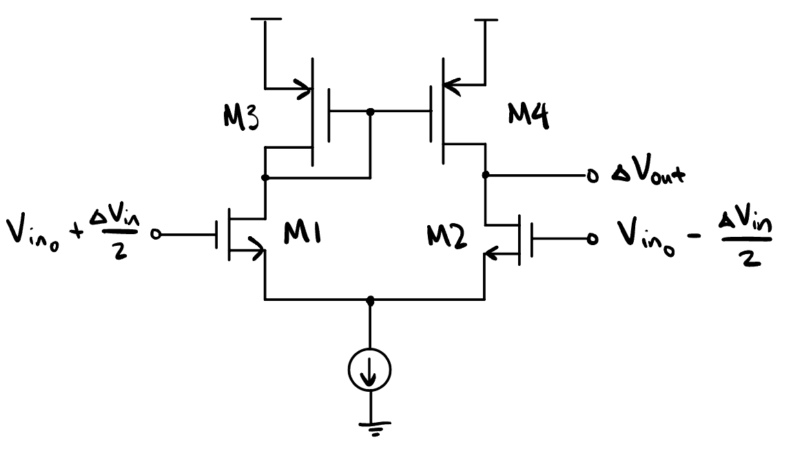
Fig. 85 Differential amplifier with current mirror load.#
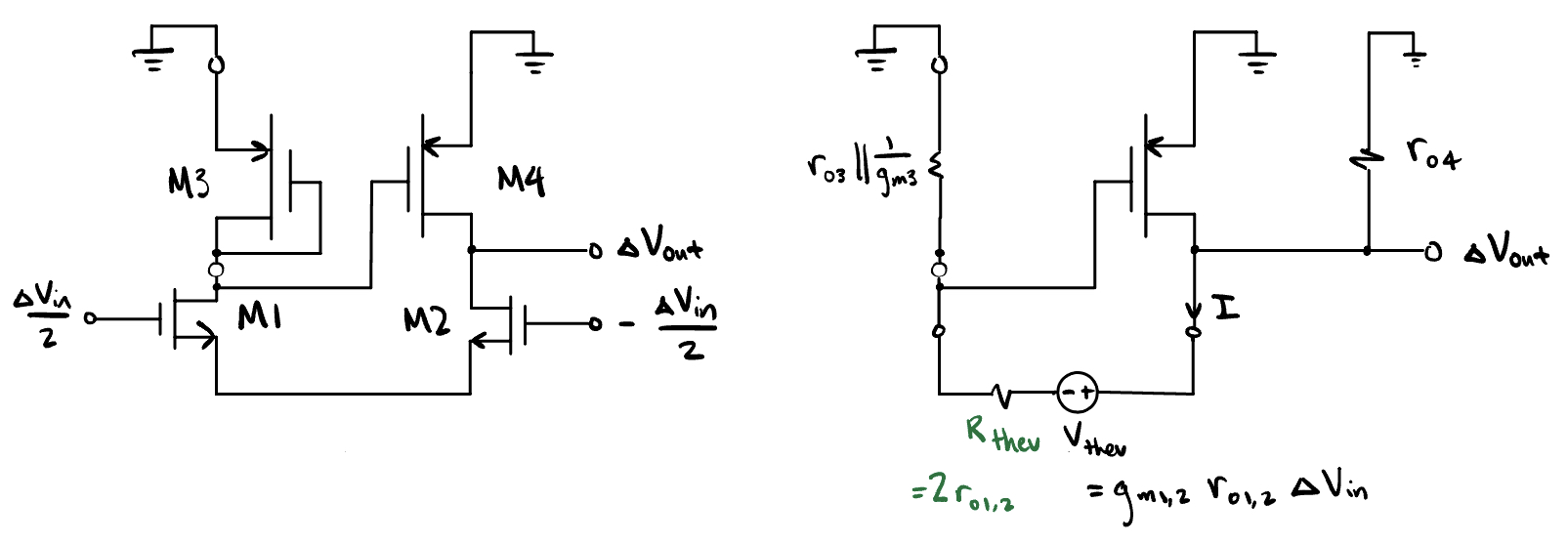
Fig. 86 Equivalent circuit model.#

Fig. 87 Voltage Thevenin equivalent circuit.#

Fig. 88 Resistance Thevenin equivalent circuit.#
Common mode response#
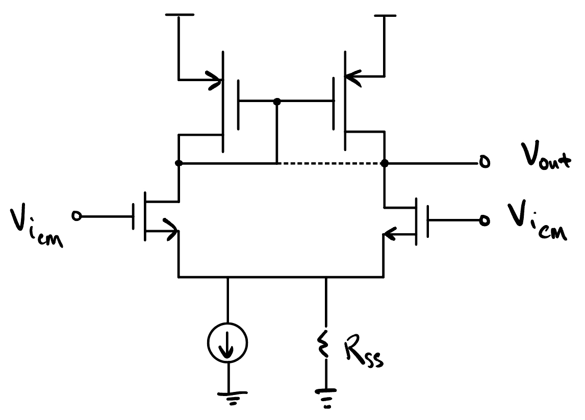
Fig. 89 Common mode circuit model.#
\(V_x = V_{\text{out}}\) if input is common.
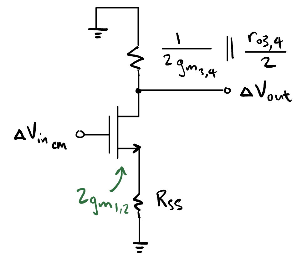
Fig. 90 Reduced common mode circuit model.#
The common mode gain, which we want to minimize, is
which is smaller than a fully-differential amplifier. If you push \(R_{\text{SS}}\) closer to infinity, it makes the common mode gain approach zero.