Common Source Amplifier
Contents
Common Source Amplifier#
Large-signal behavior#
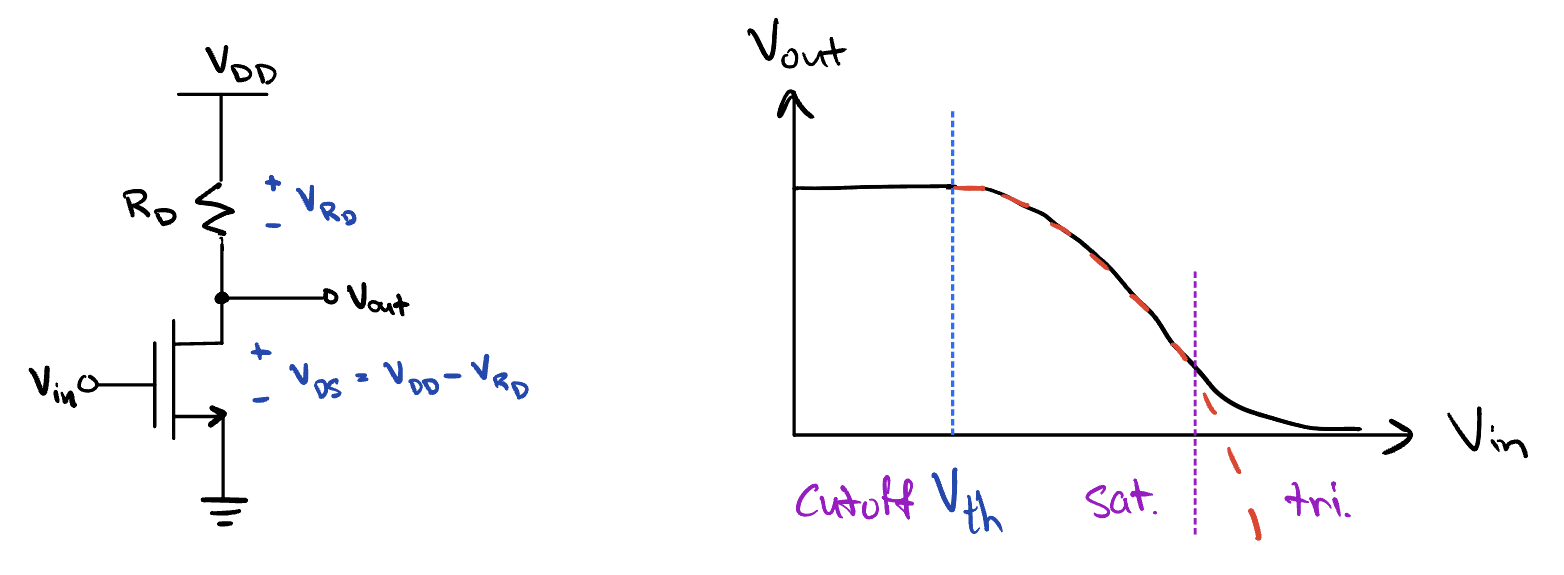
Fig. 26 Common-source amplifier and large-signal behavior.#
As \(V_{\text{th}}\) begins to ramp up from zero, the MOSFET is initially in cutoff (no channel has formed). As the saturation regime is reached, the current begins to increase quadratically (\(I_D \propto (V_{\text{in}} - V_a)^2\)). Continuing to increase \(V_{\text{th}}\) will eventually put the MOSFET into the triode regime (when \(V_{\text{GS}} - V_{\text{th}} \gt V_{\text{DS}}\)). Once you hit that point, \(I_D\) no longer increases quadratically. The max slope is therefore somewhere between saturation and triode. To achieve the maximal amplifier gain, you’d bias around that point.
Small signal gain#
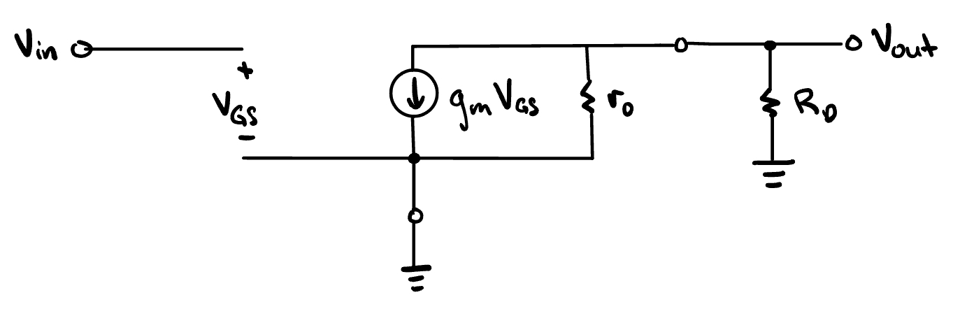
Fig. 27 Small-signal gain.#
The gain is given by
If \(R_D = \infty\),
In modern processes, this gain is on the order of -10 and \(r_o \gg 1/g_m\).
You use a large \(R_D\) to maximize gain, but this moves the transistor’s bias point closer to triode. The output swing decreases, and the gain varies with input bias voltage.
CS with NMOS load#
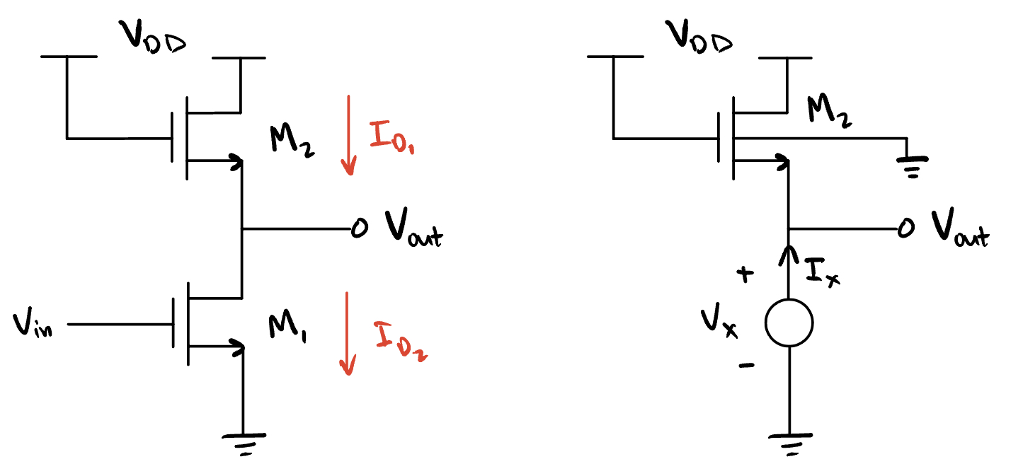
Fig. 28 CS w/ NMOS load.#
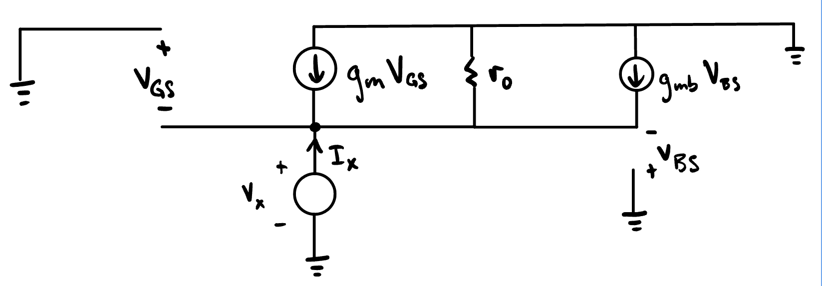
Fig. 29 Small-signal model.#
For this model, we assume that \(g_m r_o \gg 1\) and \(r_o \gg 1/g_m\).
The current \(I_x\) is given by
Also,
The gain is given by
The gain doesn’t vary with input bias voltage. It does, however, have limited swing.
In this design,
Gain is more stable across process variations.
Usually the gain is smaller compared to the previous topology.
Gain is independent of input bias.
CS with PMOS diode load#
Also known as a “diode connected transistor.”
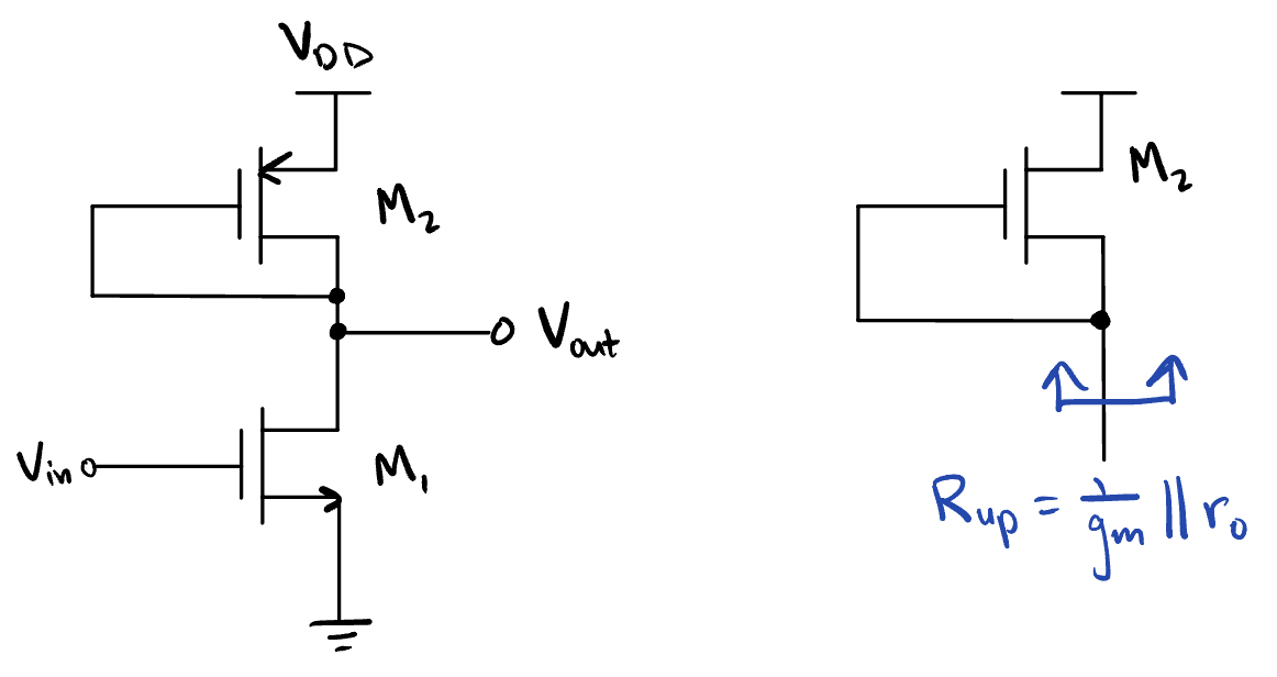
Fig. 30 Circuit diagram.#
The input resistance looking into M2 is
which is much smaller than \(r_o\) because the \(1/g_m\) term dominates in parallel.
The gain is given by
We can cancel \(I_{D1}\) and \(I_{D2}\) on the second line above if we assume a strong inversion. The gain again doesn’t vary with input bias voltage, but has limited swing.
CS with PMOS load#
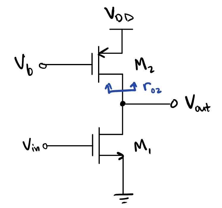
Fig. 31 Circuit diagram.#
In this configuration, the input resistance looking up is
The gain is given by
This design is
Dependent on process, voltage, temperature (PVT) variation
Much higher gain than earlier architectures.
This looks very similar to the circuit with a resistor load above \(V_{\text{out}}\). There are differences, however.
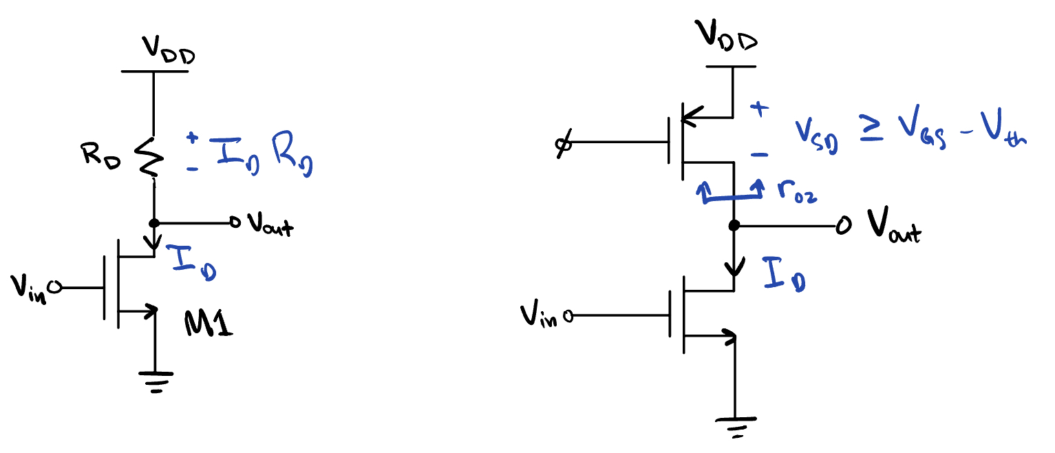
Fig. 32 Difference between resistor load and MOSFET load.#
\(r_{o2}\) can increase without driving M1 into triode. In the first case (left), a large \(R_D\) causes a large voltage drop \(I_D R_D\) which moves M1 closer to triode. In the second case (right), a big \(r_{o2}\) doesn’t change \(V_{\text{SD}}\). Therefore, M1 can stay far away from triode; the voltage drop is NOT \(I_D r_{o2}\).
Warning
You cannot multiply a large signal current with a small signal resistance.
Summary
As \(R_D\) increases, \(V_{\text{out}}\) decreases, which forces M1 into triode.
CS with source degeneration#
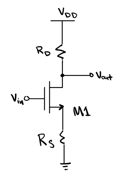
Fig. 33 Common source amplifier with source degeneration.#
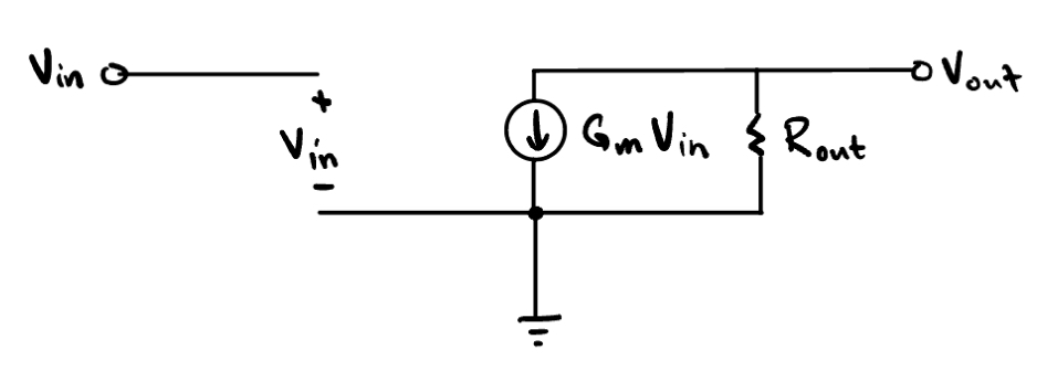
Fig. 34 Generalized amplifier model.#
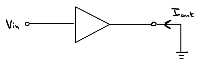
Fig. 35 Small signal ground.#
We can short the output to ground, applying \(V_{\text{in}}\) and observing \(I_{\text{out}}\), as shown in Figure 35. Doing so yields
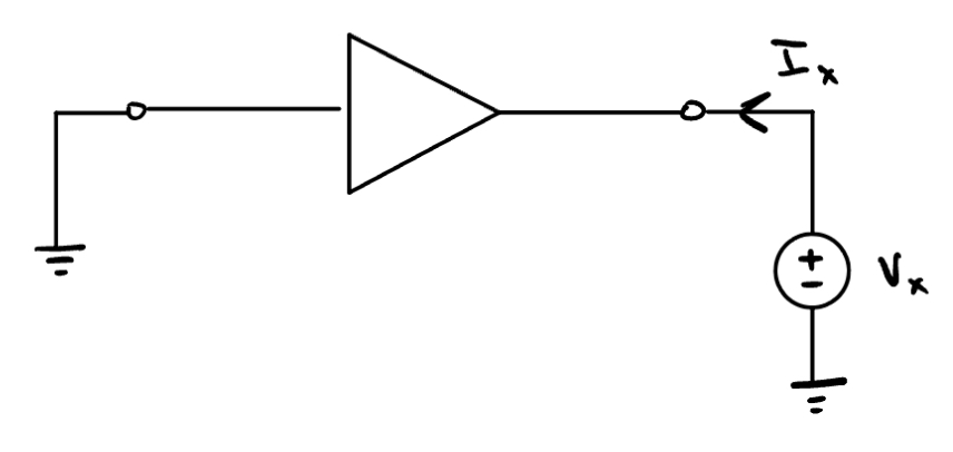
Fig. 36 Apply a test voltage.#
We can now ground the output. Apply \(V_x\), a test voltage, to the op amp and observe \(I_x\), as in Figure 36. Doing so yields
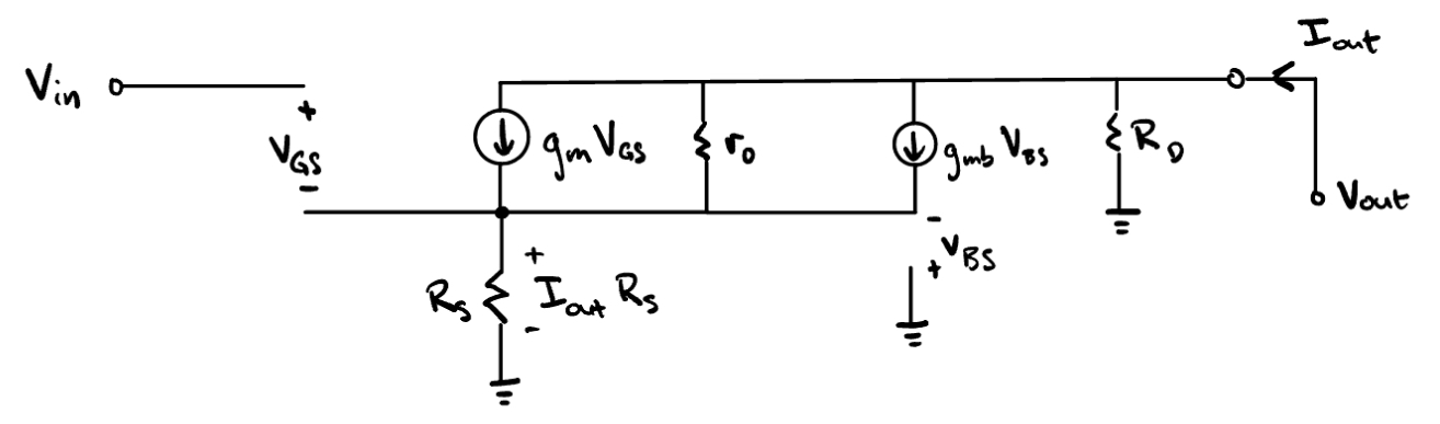
Fig. 37 CS with source degeneration small-signal model.#
Lots of equations from page 16 of the notes.

Fig. 38 Input resistance model.#
Summary
The gain of the common source with degenration is guaranteed to be less than a common source amplifier alone.
CS with degeneration is more robust over PVT than common source. Process is parameterized by variables like \(\mu\), \(c_{\text{ox}}\), etc. The voltage supply can also vary.