Common Drain Amplifier
Contents
Common Drain Amplifier#
This configuration is also known as the source-follower because the source voltage follows the gate voltage.
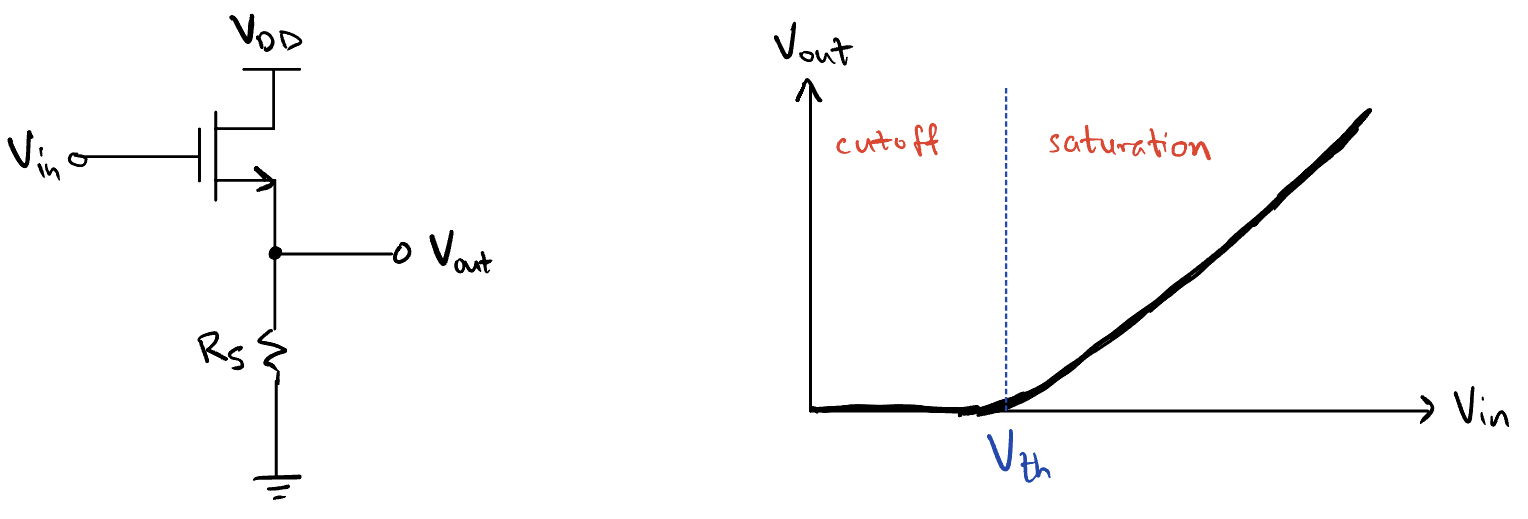
Fig. 39 Large-signal behavior.#
Small signal gain#
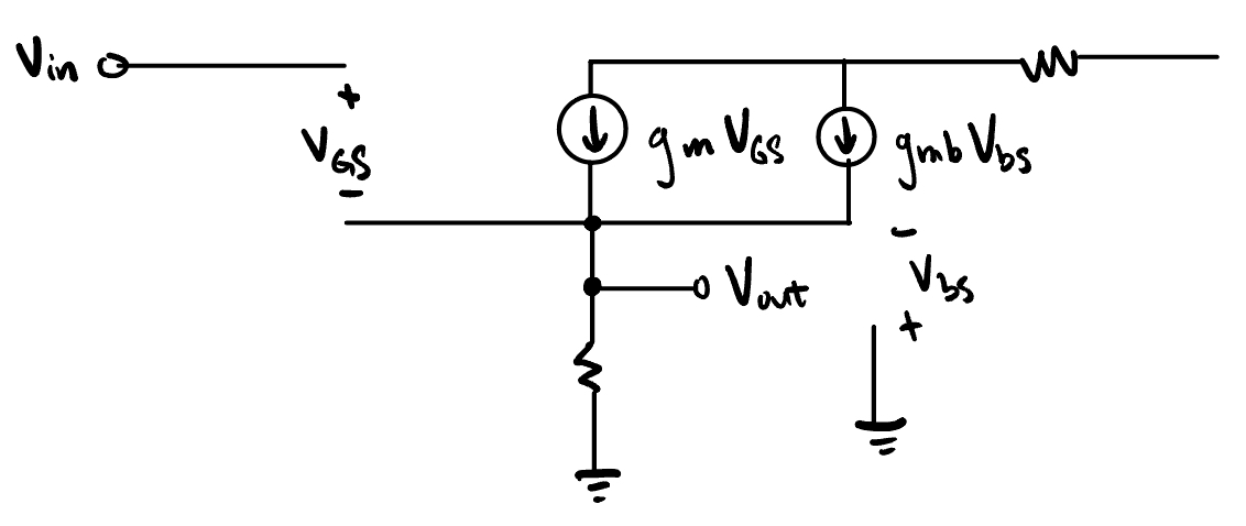
Fig. 40 Small-signal circuit model.#
Eliminating body effect#
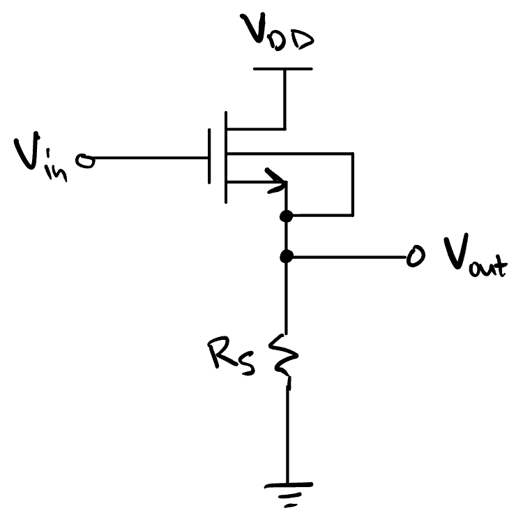
Fig. 41 Eliminating body effect by tying the bulk to source.#

Fig. 42 The triple well.#
Notes about the triple well:
✅ The gain is approximately one.
❌ It requires a lot of area on the chip (large footprint).
❌ The process needs to support a triple well.
❌ Capacitance between n-p regions means more source capacitance.

Fig. 43 Solving for the output resistance.#
Full equation#
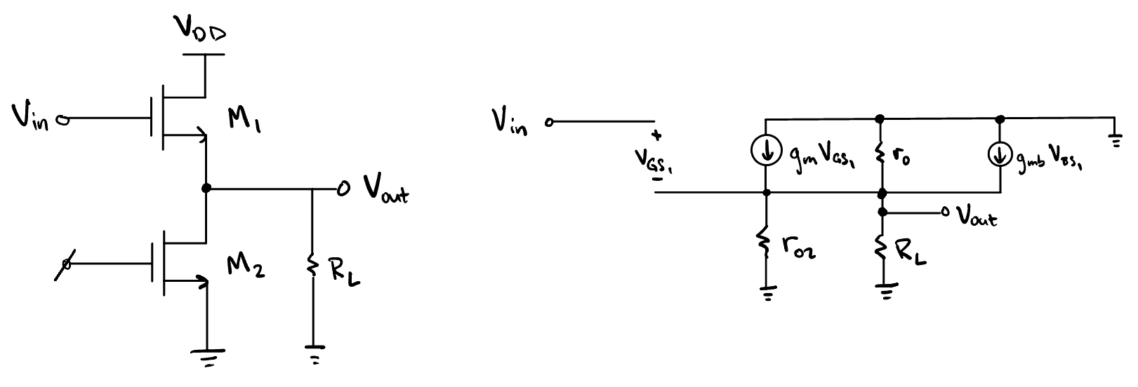
Fig. 44 Full equation.#
The gain is given by
You want to eliminate the \(1/g_{m_{1}}\) term in the denominator, if possible. It is easy to drop if the preceding term is large.
In this case, to maximize gain, you must maximize \(r_o\).
Summary
The common drain amplifier is good for driving large loads off-chip. For example, you’ve done your amplification in previous stages and can afford to attenuate a bit in exchange for low output resistance.