Differential Pair
Contents
Differential Pair#
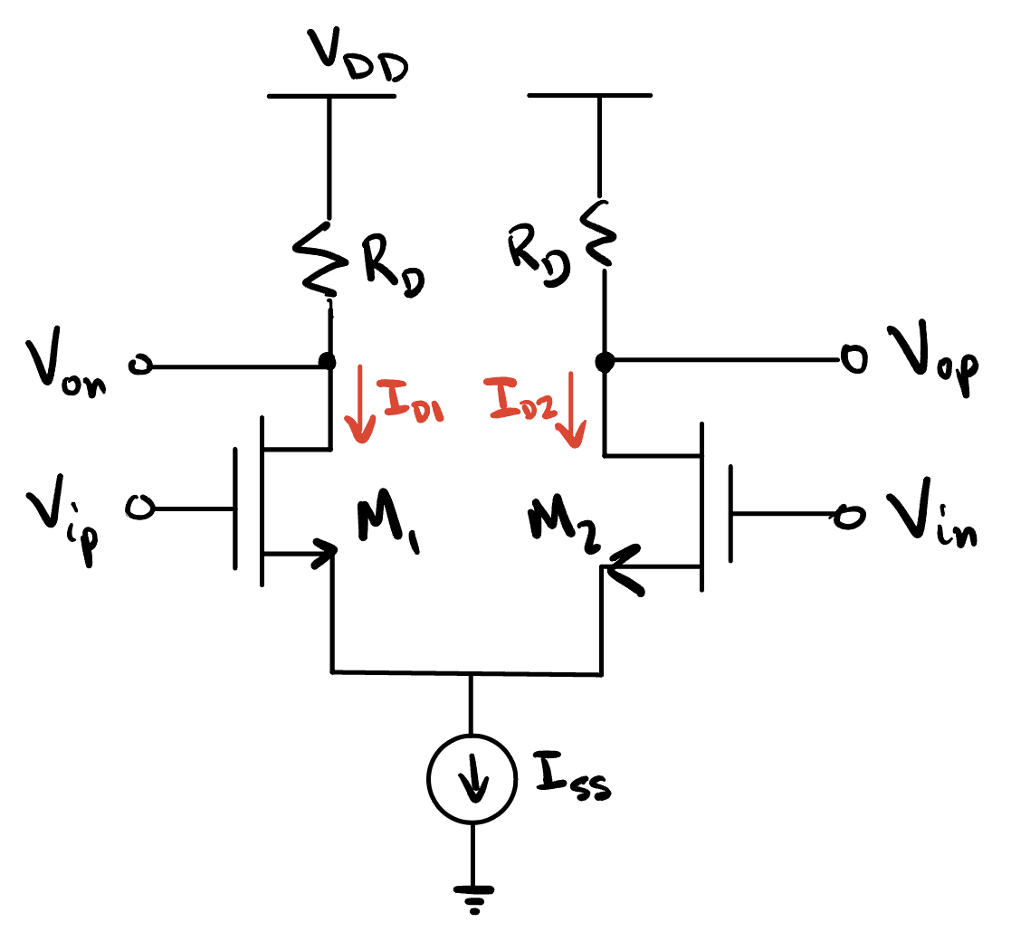
Fig. 63 Differential-pair amplifier circuit.#
Large-signal differential behavior#
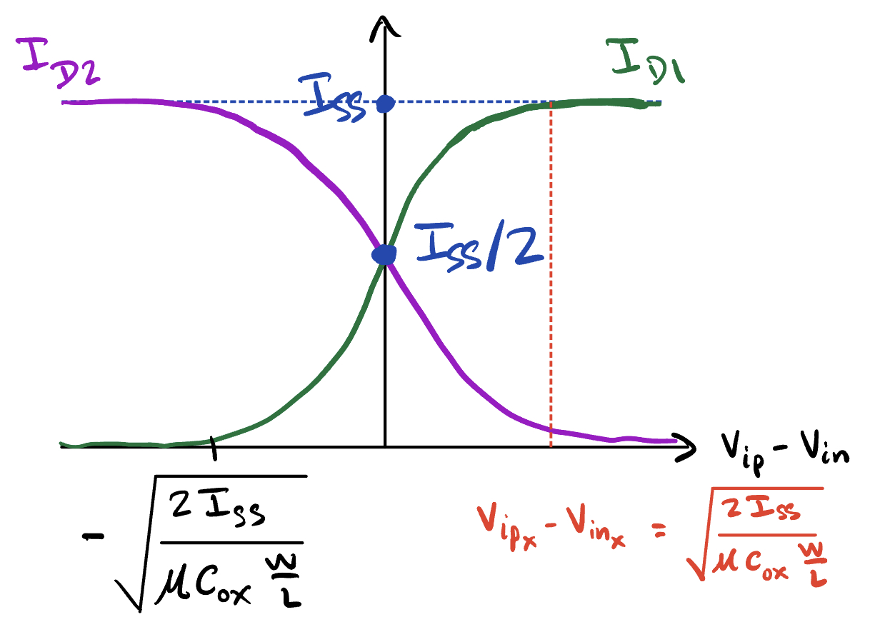
Fig. 64 Current response to differential input.#
The x-axis above is the difference between \(V_{ip}\) and \(V_{in}\). They could both be at 3V, for example, but their difference is what matters. At the critical points on the left and right side, all the current gets steered to one side.
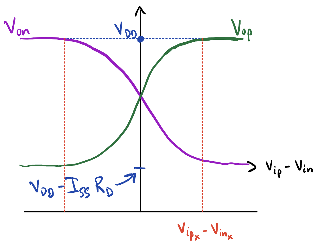
Fig. 65 Voltage response to differential input.#
The voltage tracks the current, but notice that it never reaches zero.
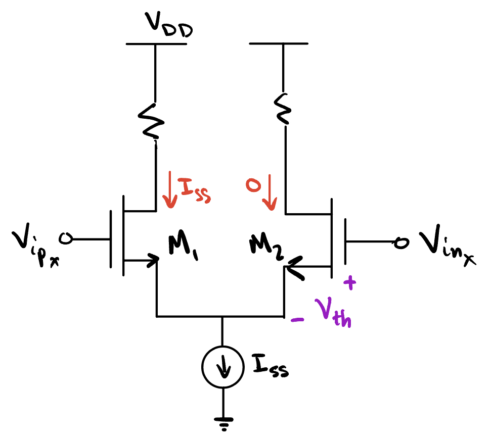
Fig. 66 Voltage response to differential input.#
What happens if M2 is “just off?” This means that \(V_{in_x} - V_{S_x} = V_{\text{th}}\). Well,
And, using the critical point from Figure 64,
Substituting (10) into (11), we get
As we approach \(V_1\), the slope (or the gain) will approach zero. So don’t get close to it!
Design Tip
To accept a wider input swing (amplifier, op amp):
Increase \(I_{SS}\), decrease \(W/L\) (but \(V_{GS}\) must increase which consumes more headroom).
To steer current more abruptly (digital logic, small input range, comparator):
Decrease \(I_{SS}\), increase \(W/L\) (but parasitic capacitance increases, making it slower).
Large-signal common-mode behavior#
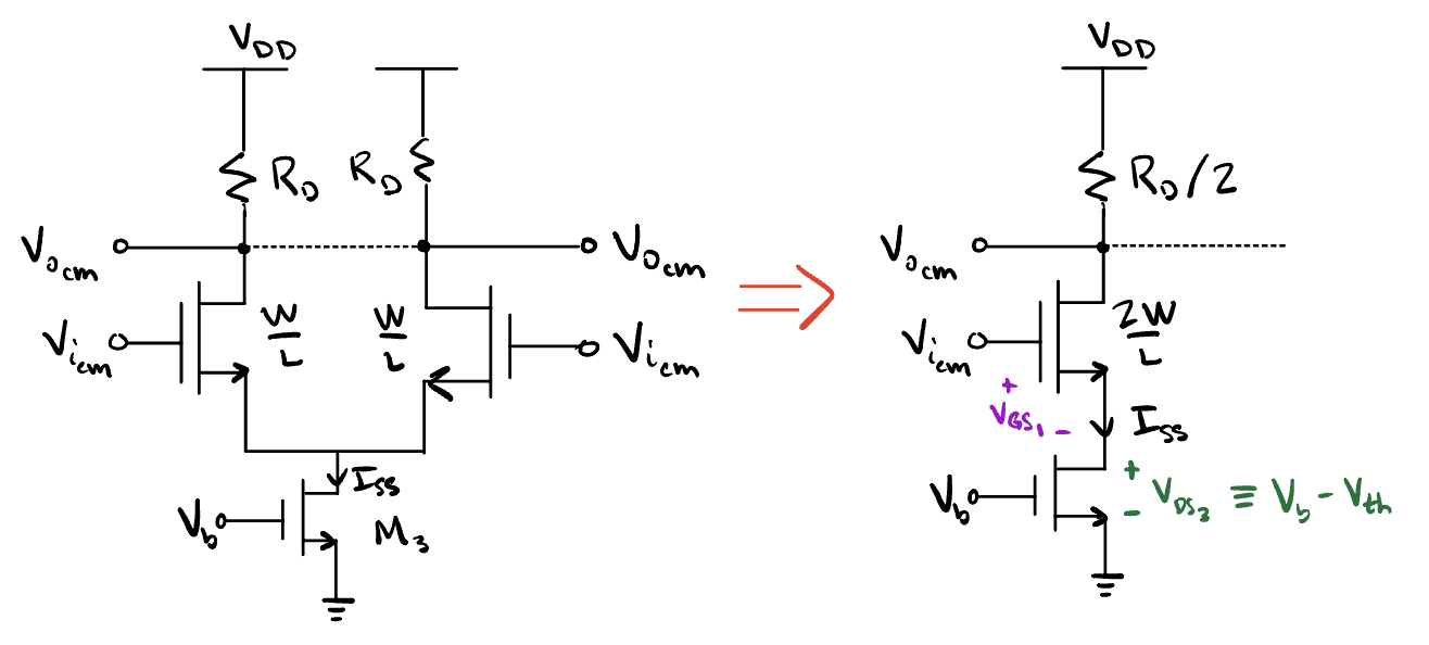
Fig. 67 Common-mode input equivalent circuits.#
In the above circuits, M3 acts as a current source. The virtual wire (indicated by the dashed black line) exists because, by symmetry, the outputs should have the same voltage for matching inputs (common mode signals).
The common mode noise is defined as (see Figure 67)
where
Note
It is possible for a MOSFET to be in triode without conducting any current.
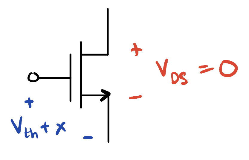
Fig. 68 Circuit in triode with no current flowing because \(V_{DS} = 0\).#
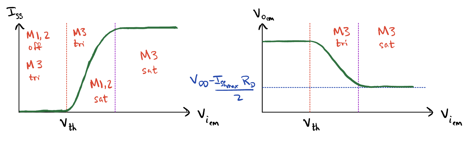
Fig. 69 Common-mode current and voltage behavior.#
We want to operate where \(I_{SS}\) is approximately constant (so, in the third regime in the above figure where both M3 is in saturation). This helps prevent \(g_m\) from really changing.
Small-signal gain#
Under the condition that \(\lambda = 0\), \(\gamma = 0\).
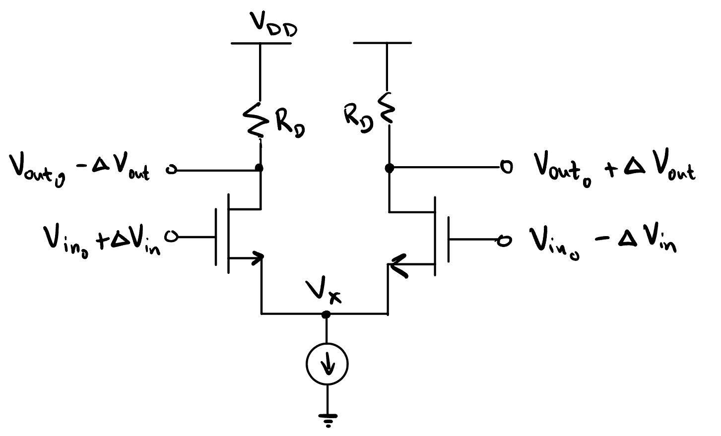
Fig. 70 Small-signal circuit model.#
In the above configuration, \(V_x\) doesn’t change since the circuit is symmetric. \(\Delta V_{\text{in}}\) is the common perturbation.
Therefore, \(V_x\) is small-signal ground.
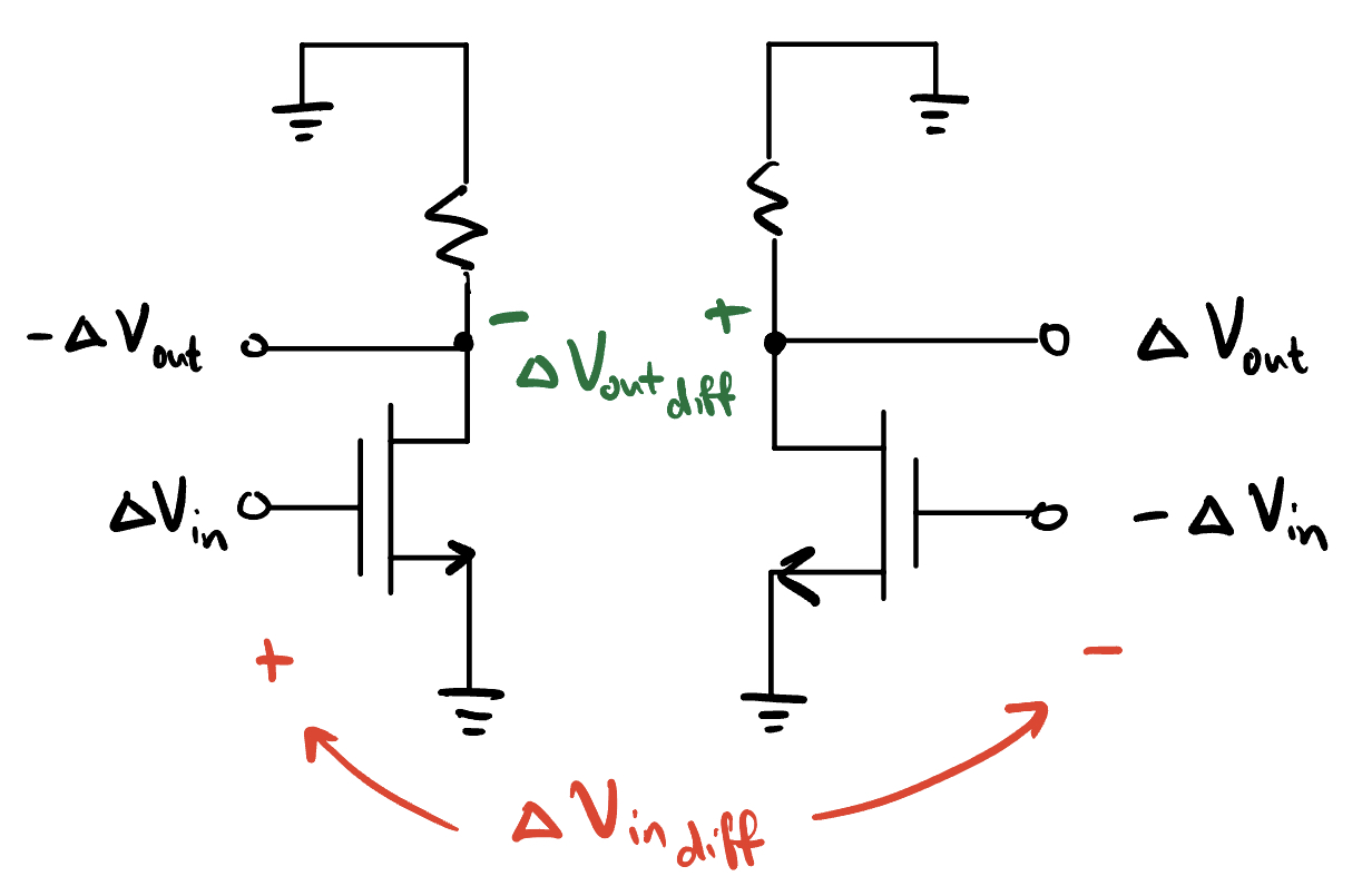
Fig. 71 Reduced circuit in the small-signal model.#
The gain is given by
Small-signal common-mode response#
Under the condition that \(\lambda = 0\), \(\gamma = 0\).
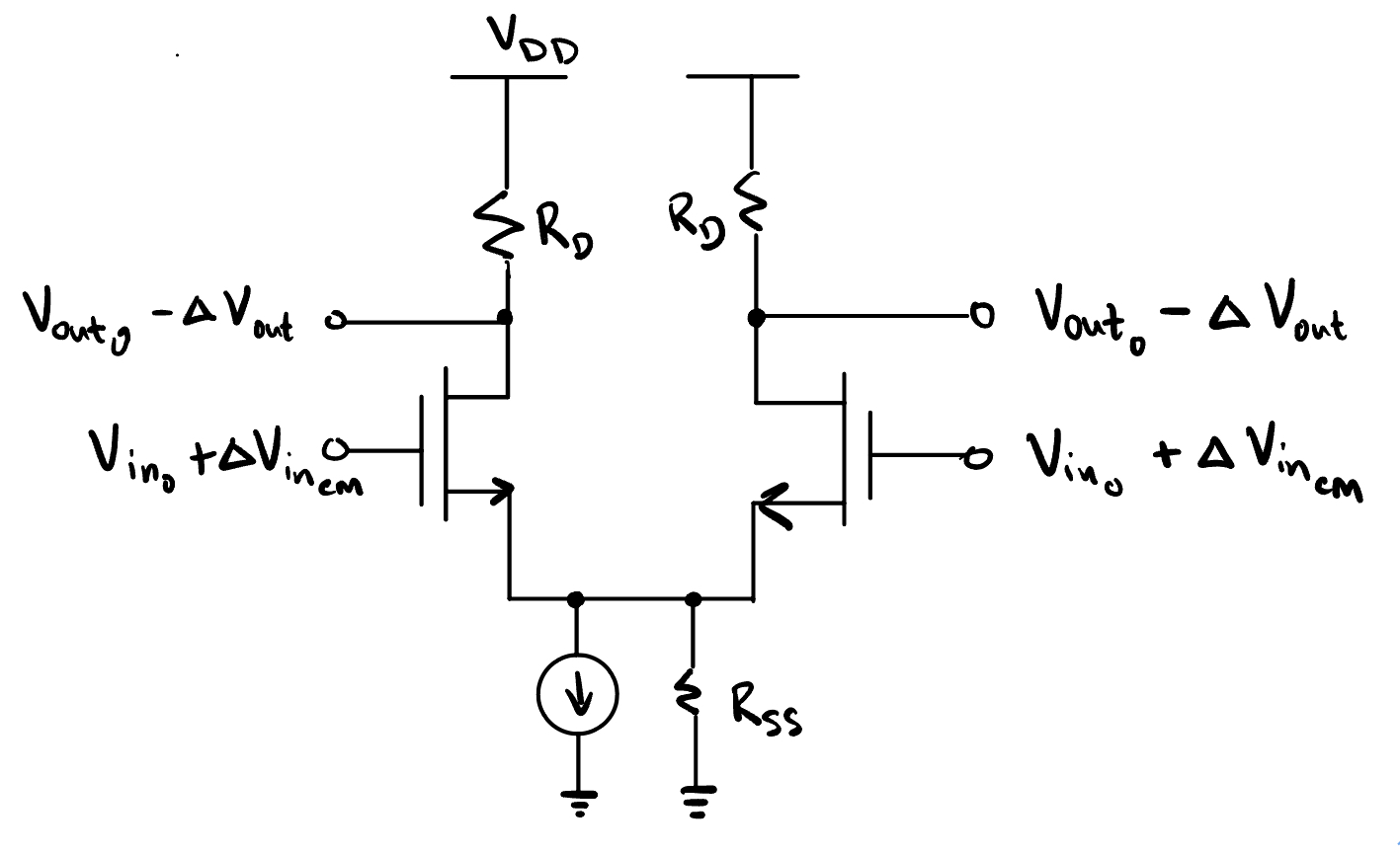
Fig. 72 Common-mode small-signal circuit model.#
Note the current source and resistor now at the source of the MOSFETs. This is the Norton equivalent circuit model for a current source. In a small signal analysis, the current source is an “open circuit.”
Recall that we want to make the differential gain as big as possible, but we want the common mode response as small as possible.
The circuit in Figure 72 reduces to the following.
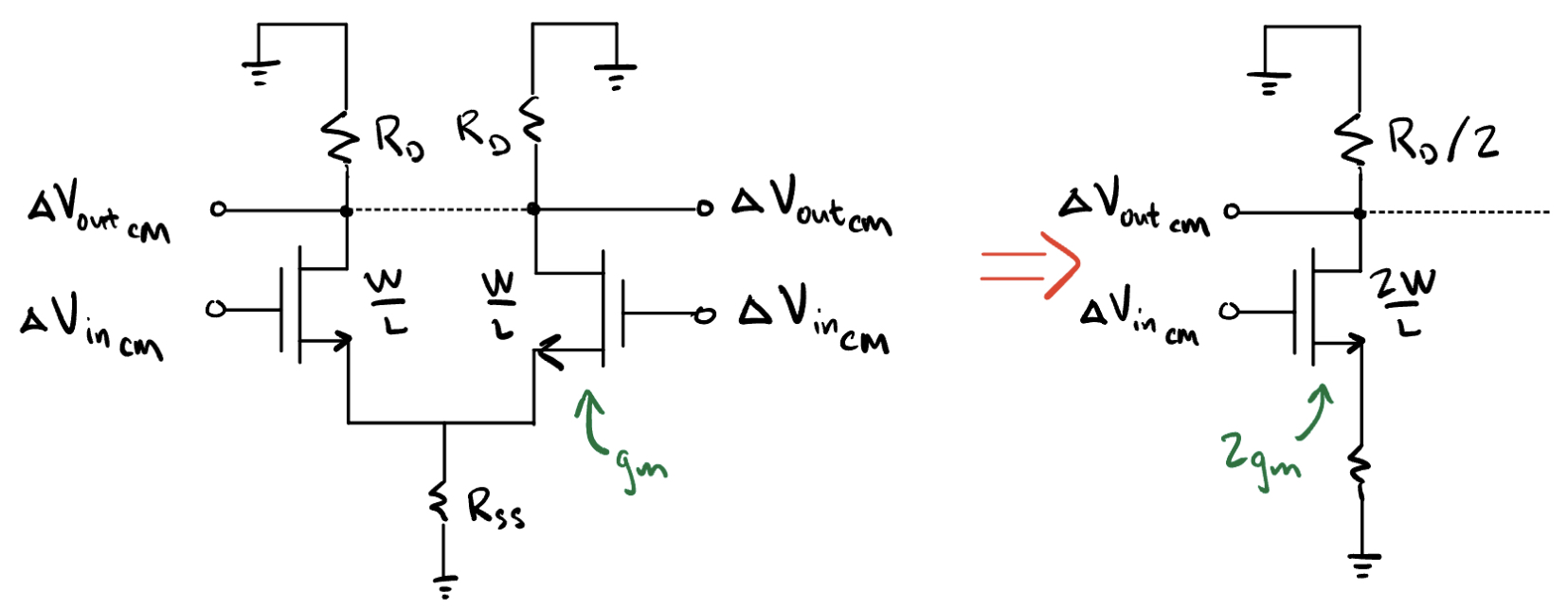
Fig. 73 Reduced common-mode small-signal circuit model.#
The common-mode input to common-mode output gain, which we want to minimize, is
Note that \(g_{\text{m 1,2}}\) comes from \(2W/L\), hence we get \(2 g_m\).
Hence, we should use a large \(R_{SS}\) to reduce common mode gain (and use a non-minimum \(L\) for fast transistor).
Good input common mode rejection is the reason to use \(I_{SS}\) (rather than grounding the source nodes).
Takeaways
⬆️ \(R_{SS}\)
⬇️ \(R_D\)
Use big L for M3 to increase \(R_{o3}\) (\(R_{SS}\))
If there is a mismatch in \(R_D\):
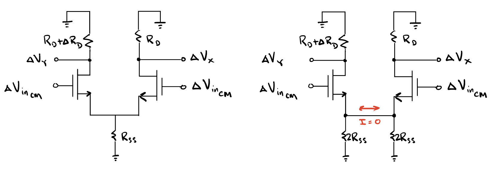
Fig. 74 Reduced common-mode small-signal circuit model.#
The outputs (for a common-mode input) are given by
and
Then,
and the commmon-mode-to-differential-mode conversion gain is
It is evident that you should use a large \(R_{SS}\) to decrease \(A_{\text{CM-DM}}\).
One useful quantity is the common mode rejection ratio (CMRR), which is defined as
Typical Implementations#
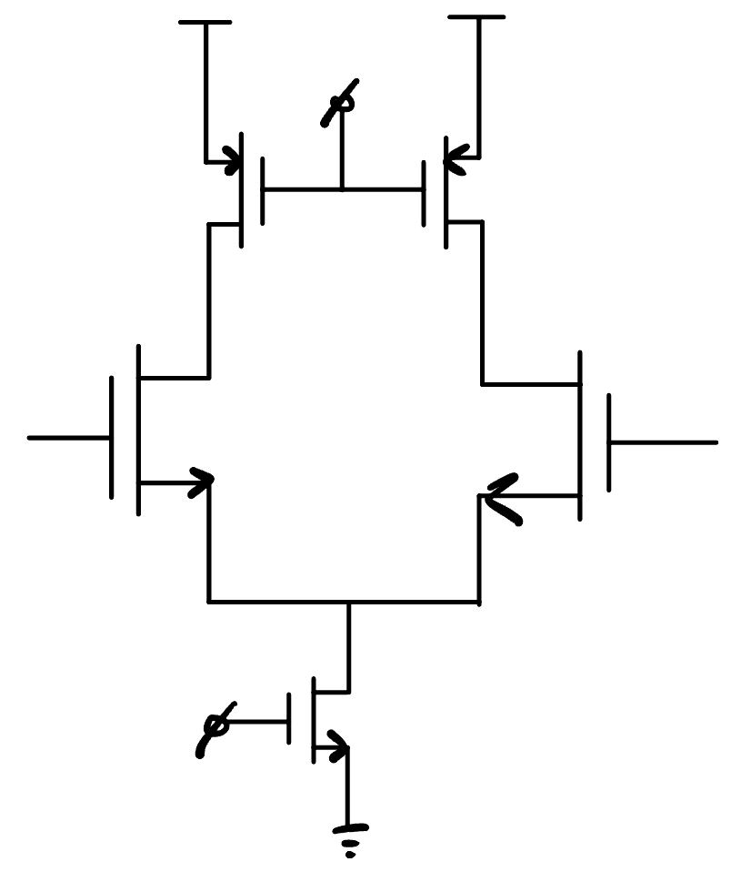
Fig. 75 PMOS load.#
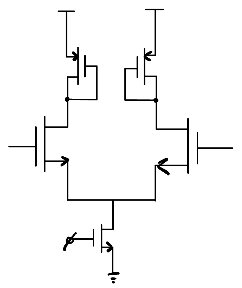
Fig. 76 Diode-connected PMOS load.#