MOSFET Device Physics
Contents
MOSFET Device Physics#
A few definitions:
- \(V_{DS}\)
Voltage from drain to source.
- \(V_{GS}\)
Voltage from gate to source.
Regimes of Operation#

Fig. 1 Physical model of a transistor and its circuit representation.#
In this configuration, the transistor is off. The p-substrate is almost an insulator, and the transistor doesn’t conduct. There’s no current, because there’s nowhere for it to go!

Fig. 2 The gate voltage is less than the drain voltage, and the transistor is off.#
The gate voltage is rising, repelling p-type carriers away from the channel.
In this situation, the electrons are still all attached to their atoms’ nucleus and are not moving. The negative ions are forming a depletion region; there are no free carriers, but the net charge of the region in the material is negative.
Since there are no holes or carriers to conduct electrons, the current is still zero.
- doping
the introduction of impurities into a semiconductor crystal. It can leave open holes for electrons to fill in the crystal lattice, or have too many electrons to fill the valence shell. This means free carriers are introduced, but since the total number of protons and electrons are equal, it still leaves the material electrically neutral.

Fig. 3 The gate voltage is greater than the drain voltage, the transistor is on, and current starts to flow.#
The gate voltage is now greater than the threshold voltage, and the electrons form a channel close to the gate. Free electrons can detach from their nucleus and flow. Current flow from the drain to the source is now non-zero.

Fig. 4 3D view of a MOSFET with length and width dimensions labelled.#
Obviously, when \(V_{\text{GS}} \lt V_{\text{th}}\), \(I_D = 0\). When the gate voltage surpasses the threshold voltage, the current through the drain is given by
where \(\mu\) is the electron mobility and \(c_{\text{ox}}\) is the gate oxide capacitance per unit area.
The larger \(L\) is, the smaller \(I_D\) is. Conversely, the wider \(W\) is, the greater \(I_D\) is.
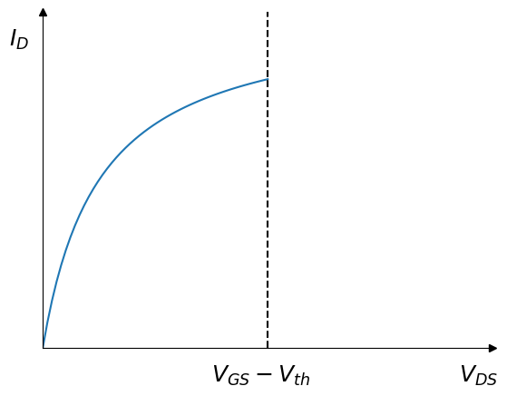
Fig. 5 Current vs. drain voltage (assume \(V_{GS} \gt V_{th}\)).#
Note that in the above plot, the current is initially linear until the second term catches up. At \(V_{\text{DS}} = V_{\text{GS}} - V_{\text{th}}\), pinchoff occurs.

Fig. 6 3D view of a MOSFET with length and width dimensions labelled.#

Fig. 7 3D view of a MOSFET with length and width dimensions labelled.#
The channel is “pinched off.” This means a further increase of \(V_{\text{DS}}\) does not increase \(I_D\).
Note
So, is \(I_D = 0\)?
No; the super strong electric field in the pinched off region causes any electron entering that field to be swept away (an across).
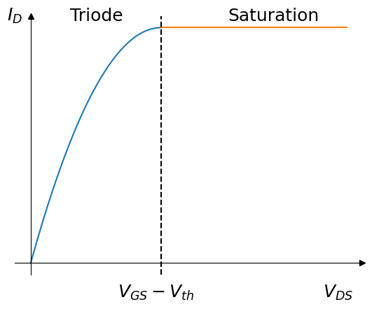
Fig. 8 Current vs. drain voltage (assume \(V_{GS} \gt V_{th}\)).#
Analog designers mostly work in saturation, while digital designs usually operate in triode (and off).
Current Equations#
The current equations for triode and saturation are
and
respectively.
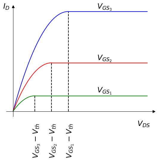
Fig. 9 Current vs. drain voltage (assume \(V_{GS} \gt V_{th}\)).#
The lower \(V_{\text{GS}}\), the earlier the transition happens.
\(V_{\text{th}}\) doesn’t usually change; it’s typically around \(0.5 \text{V}\).
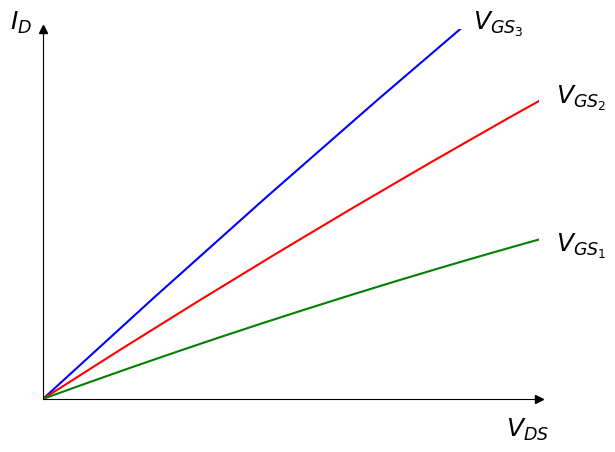
Fig. 10 Current vs. drain voltage (assume \(V_{GS} \gt V_{th}\)).#
The current resembles the I-V curve of a resistor when biased in this region.
In triode,
if \(V_{\text{GS}} - V_{\text{th}} \gg V_{\text{DS}}\), and the resistance is given by
because resistance is defined as the inverse of the slope of the IV characteristic curve.

Fig. 11 A MOSFET in triode can be used as a voltage-controlled resistor.#
Transconductance#
- transconductance
Transconductance is an expression of the performance of a field-effect transistor (FET). In general, the larger the transconductance figure for a device, the greater the gain (amplification) it is capable of delivering, when all other factors are held constant. For a FET, transconductance is the ratio of the change in drain current to the change in gate voltage over a defined, arbitrarily small interval on the drain-current-versus-gate-voltage curve. The unit is the siemens.
Transconductance in saturation is given by:
\(g_m\) is the slope at some point \(V_{\text{GS}}\).
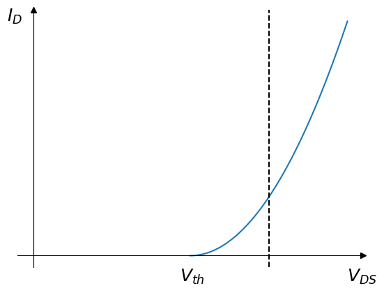
Fig. 12 \(g_m\) is the slope at some point \(V_{\text{GS}}\).#
Channel-length modulation#
Channel-length modulation (CLM) is a second order effect that doesn’t affect the IV curve as strongly. The channel length \(L\) becomes smaller as \(V_{\text{DS}}\) increases. As you increase \(V_{\text{DS}}\), the pinchout zone gets a bit smaller, increasing \(I_D\). Sometimes we ignore this effect.
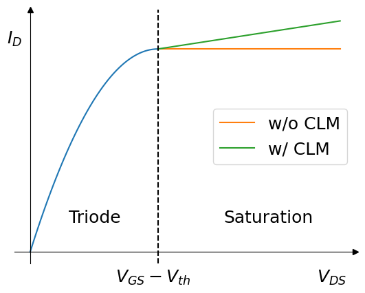
Fig. 13 Current with and without channel-length modulation.#
The corresponding equation when in saturation is
and its slope is
where \(\lambda\) is a process parameter that varies with transistor length.
The smaller the architecture, the more pronounced CLM effects will be. This is bad for analog design! If you want a smaller slope, make \(L\) bigger (or have a smaller current)!
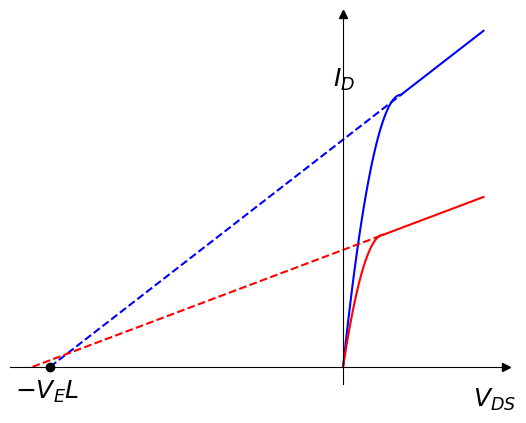
Fig. 14 The per-channel-length early voltage.#
If \(V_E L \gg V_{\text{DS}}^{'}\):
and therefore
Body effect#
Page 5
Subthreshold conduction#
Page 5
MOSFET capacitance#
Page 6
MOSFET as a varactor#
Page 7